
Detail
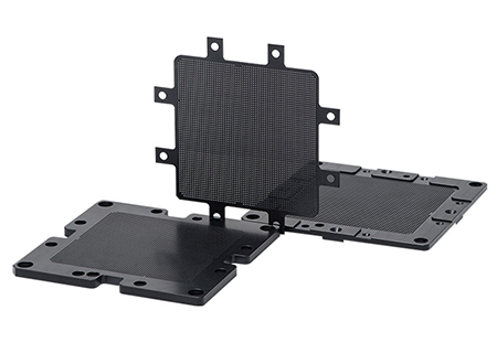
Test socket guide plate micromachining represents the pinnacle of high-precision technology in the semiconductor testing industry. By harnessing advanced techniques, this process expertly navigates the complex geometries of cutting-edge semiconductor architectures. In a world where nanometer-scale precision is critical, micromachining stands as the leading solution, ensuring flawless alignment and impeccable testing fidelity. This technology not only meets the demands of today’s tech-driven world but also lays the foundation for future AI-powered advancements in precision and performance.
Test Socket Guide Plates Micro-Machining Results & Achievements
- Product Size: 0.7 x 82 x 82 mm
- Deformation: ± 0.01 mm
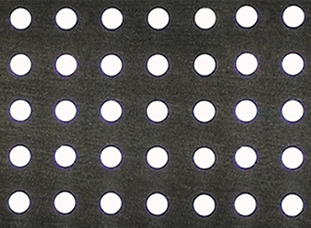
- Micropore Enlargement: No burrs after magnifying micropores by 100x
Our precision micro-machining ensures flawless results, with minimal deformation and perfect surface quality, even after significant magnification of the micropores.


With 20 years of experience in engineering plastic processing, we provide solutions to any challenges you may encounter, including difficult issues such as deformation, concentricity, and positioning, particularly in test socket applications.
Precision We Achieve
We are capable of milling Ø 300 μm round holes with a 350 μm pitch into challenging engineering plastics like Torlon and Vespel, with a thickness of 500 μm and an impressive cycle time of just 0.6 seconds. Additionally, Torlon can accommodate a countersunk step hole, precisely measured at Ø 3.0 mm with a 1 mm depth and Ø 2.5 mm with a 0.8 mm depth. In contrast, Vespel demonstrates our expertise with step holes ranging from Ø 400 μm to Ø 650 μm, with a pitch of 750 μm, and through holes precisely drilled to Ø 200 μm, with a depth of 650 μm.


If you currently have a test socket guide plate micromachining project, we would be happy to discuss how we can achieve outstanding results together, with a focus on precision technology.


